-
Mob.:
+86 135 9088 4785
+86 135 9088 4785
The design principle of the light guide plate originates from the liquid crystal display of notebook computers and is a high-tech product that transforms linear light sources into the surface light sources. Optical grade acrylic (PMMA)/PC as the substrate, the use of LCD display and laptop backlight module technology, through the high light transmission rate of the light guide point, by computer calculation of the light guide point, so that the light guide plate light refraction into the surface light source uniform light state manufacturing molding.

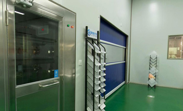
The product adopts the combination of spectral analysis principle and digital UV printing technology and is made under constant temperature, humidity and dust-free environment. With the ultra-thin, ultra-bright, uniform light guide, energy saving, environmental protection, no dark area, durable, not easy to yellowing, installation and maintenance is simple and fast.
Flat plate: The light guide plate is rectangular from the light inlet.
Wedge-shaped plate: also known as oblique plate, from the light into the side of a thick side for the thin side of the wedge (triangle) shape.
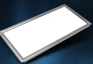
Printed: After the completion of the shape of the light guide plate processing, printed dot in the reflective surface, and divided into IR and UV two.
Non-printing type: the dot will be directly formed on the reflective surface when forming the light guide plate. Also divided into chemical etching (Etching), precision mechanical engraving method (V-cut), light micro-shadowing method (Stamper), and internal diffusion.
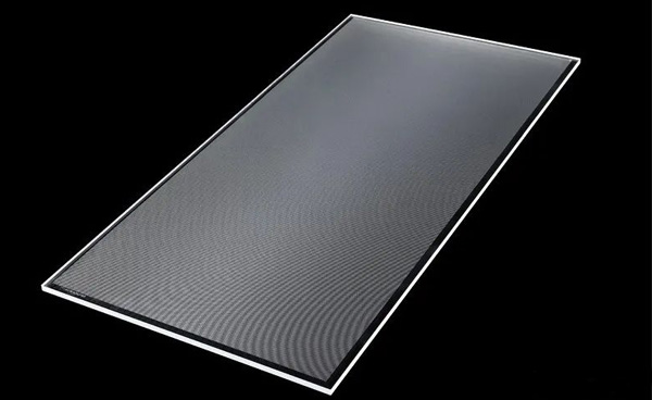
Side entry type: the luminous body (lamp or LED) placed in the side of the light guide plate.
Straight down type: the luminous body (lamp or LED) placed in the light guide plate below.
Injection molding: The optical grade PMMA particles are injected into the mold with high temperature and pressure by injection molding machine to cool and shape.
Cutting and forming: The optical grade PMMA sheet is cut after the cutting process.
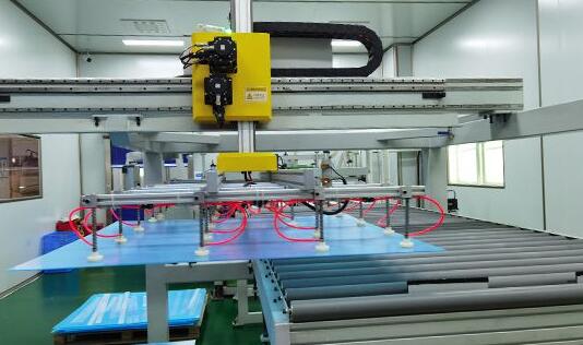
● Can be cut to the required size or spliced, simple process and easy to make.
● High light conversion rate (more than 30% higher than traditional panels), uniform light, long life span, can be used normally for more than 8 years indoors, safe, environmentally friendly, durable and reliable for both indoor and outdoor use.
● High luminous efficiency and low power consumption under the same area luminous brightness.
● Can be made into shaped shapes, such as circles, ellipses, arcs, triangles, etc.
● Thinner products can be used to save costs under the same brightness.
● Can use any light source, point line light source to do the conversion of the surface light source, the light source including LEDCCFL (cold cathode lamp tube), fluorescent tube, etc.
Luminosity: High luminosity is required, for example, 1600nit for notebooks; 3000~6000nit for monitors
Uniformity: 75% for black and white LCD modules and 80% for color LCD modules
Power consumption: low power consumption is required, generally 3~3.5mA for Lamp tube current.
Weight: This feature is quite an important point of consideration for backlight panels for portable computers, in order to seek lightweight, in addition to the light guide plate from the original flat plate to wedge type (wedge type), and towards a thinner direction of development (wedge type thickness has required 2.0 ~ 0.7mm). Although weight is not an important issue for desktop LCDs, the weight of the light guide will become a key consideration in module design when the display is developed in a larger size.
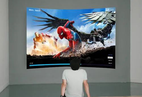
Application of Optical Materials in TV Displays
The above four characteristics are the main basis for evaluating the performance of backlight panels. But in fact, due to the conflicting requirements between these requirements, such as low power consumption and high luminance, light and thin light guide plate, and high light guide efficiency, it will be difficult to make each characteristic reach the maximum, so how to achieve the maximum total performance is a major test of backlight board design.
Since the 90's, science and technology continue to develop, the production method of light guide plate slowly improved, derived from different from the early printing type production, as opposed to it, we call "non-printing type".
Injection molding: It is to fill the molten forming material into the closed mold with high pressure, which requires the light guide and the microstructure to be completed simultaneously in the injection molding, and the mold must be made quite strong, so the mold price is also quite expensive, so it must be produced in large quantities to offset the high cost of the mold. Single-sided microstructure arrays of light guides are generally produced by injection molding process, and its bottom texture structure can be in the shape of tiny lenses, microspheres or tetrahedral angular cone prisms, etc.
Photolithography: Photolithography is the process of coating a flat silicon wafer with a layer of corrosion-resistant photoresist, and then allowing strong light to pass through the photolithography plate, where it is selectively exposed according to the graphic information of the specific layer produced; the developed photoresist is then removed, leaving a thin film with a micrographic structure on the surface of the silicon wafer. The surface roughness of the light guide plate made by photolithography is poor, and the loss of light energy is relatively large.
Doping: A transparent particle material with a scattering function is injected directly into the inside of the light guide plate during injection molding, and the effective control of light output is achieved through reasonable adjustment of the concentration of transparent particles to finally achieve high uniformity of light output. Due to the doping process is not easy to precisely control, so the injection method is suitable for the production of the small and medium-size light guide plates, for large size light guide plates will have uneven light problems.
Laser engraving: The laser engraving method is to use the computer to strictly control the laser head energy and laser head position according to the program requirements, and use the gasification method to engrave the microstructure array with a certain size on the back of the light guide plate, this method can control the depth of the scattering structure very precisely, but the efficiency is very low and not convenient for mass production.
Sandblasting: Using a sandblasting method to make a mold with a rough distribution surface, the rough distribution on the mold is transferred to the light guide plate during injection molding, the more rough surface, the stronger the scattering ability, through reasonable adjustment of the rough distribution of the surface to achieve uniform light distribution on the light output surface.
Single point diamond processing: single point diamond processing is also called nano processing technology, and its processing accuracy can reach nano-level surface roughness. It is to fix the workpiece on the precision lathe and use the natural single crystal diamond tool for fixed-point turning. First, the guide plate dies core is fixed on the rotary axis and rotated, and then the fast piezoelectric feed of the diamond fast tool is used to produce the finish. The concave and convex lens of the guide plate is processed by the fast tool feed system and then configured with ultra-precision single-point diamond equipment.

Copyright ©Kunxin New Material Technology Co., Ltd. All Rights Reserved | Sitemap | Technical Support: 